|
|
|
|
|
|
Single-ended PCB stripline structures
Application Note AP123
|
|
|
PCB transmission line structures This application note looks at the single-ended stripline structure – one of the two most popular constructions of transmission lines on PCBs. Application Note AP121 describes how controlled impedance PCBs are usually produced using microstrip or stripline transmission lines in single-ended (unbalanced) or differential (balanced) configurations. This application note considers single-ended stripline structures. As with the microstrip structure these are unbalanced line structures, i.e. the cross-section of the signal conductor is different from that of the return ground plane conductor. As with the case of the microstrip structure the characteristic impedance of the stripline structure will be a function of the physical dimensions of the trace and the dielectric constant of the PCB substrate material and dielectric thickness. Stripline Structures The stripline typically consists of a line conductor trace sandwiched between two reference planes and a dielectric material. The transmission line, i.e. the trace and planes, form the controlled impedance. The value of the impedance will be determined by its physical construction and electrical characteristics of the dielectric material:
For all practical purposes the dielectric may be regarded as homogeneous. Electromagnetic waves in a vacuum travel at the speed of light. The propagation velocity in a material is primarily dependent on the Er of the material (roughly inversely proportional to the square root of the dielectric constant of the material). Assuming a value of about 4 for dielectric constant for G-10 or FR-4 (the actual value will depend on frequency and the glass to resin ratio) the propagation velocity will approximate to half the speed of light. There are several configurations of PCB stripline:
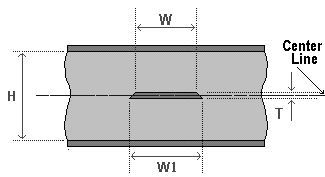
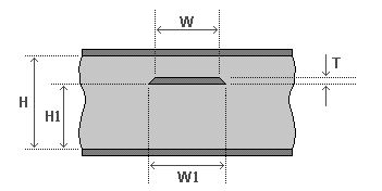
These structures are illustrated in the diagrams below. Single-ended Striplines Note that in the following diagrams the signal trace is actually trapezoidal in profile and width W refers to the trace width nearest the upper surface, width W1 refers to the trace width nearest the lower surface. A stripline differs from a microstrip in that it is a line embedded in a dielectric between two reference planes. There are two variations of stripline configuration — the centred or symmetric stripline and the offset stripline. |
|
|
Symmetric Stripline
Figure 1 Symmetric stripline |
In the symmetric stripline configuration (shown in Figure 1) the signal trace is sandwiched symmetrically, i.e. centred, between the two reference planes. This is often difficult to achieve as the laminate above and below the trace will be either C-Stage or B-Stage (core or pre-preg) material. |
|
Offset Stripline
Figure 2 Offset stripline |
In the offset or asymmetric stripline case the trace is sandwiched between the two reference planes but is closer to one plane than the other. |
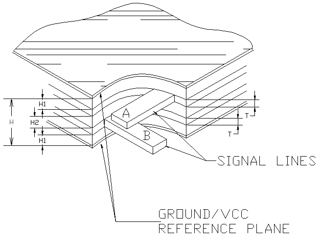
A second mirror trace may be positioned at distance H1 from the top ground plane. This structure is referred to as dual stripline — in this case the two signal conductors are sandwiched between the two reference planes on adjacent layers. These two signal layers will be routed orthogonally to minimise inter-layer crosstalk; i.e. the signal layers are made to cross at right angles so as to minimise the crossing area. The structure is then behaving as two independent offset striplines. The dual stripline structure is shown in Figure 3 below. |
|
Figure 3 Dual stripline structure |
|
|
The diagrams show the characteristic stripline impedance attributes:
The equations for characteristic impedance require complex mathematics, usually using field solving methods including boundary element analysis and are beyond the scope of this document. |
|