|
|
|
|
|
|
Characterising PCB production process for controlled impedance
Application Note AP129
|
|||
|
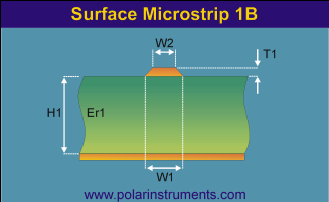
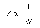
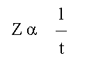
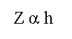
Process Characterisation The Polar field solving impedance calculators provide a good starting point for nominal values of trace width, however the powerful math behind all field solving tools which calculate impedance rely on the use of "Ideal" materials. Unfortunately in the real world life is not quite as simple. PCBs are composites of glass and resin with differing electrical characteristics and production processes will vary from one PCB fabricator to another. To fully understand your process you will need to produce test panels with many types of design in order to discover how your process differs from theory. The data you gather will help you work more closely with PCB designers to achieve maximum yields. Processing test samples with line widths down to your minimum will enable you to estimate how yields reduce with smaller line widths which will result in better cost estimates for your customers. Ideally you will produce panels of standard coupons and each coupon can contain a variety of impedances and structures. After manufacture of the test panels, you will then need to measure the actual values of impedance. Ensure that your impedance test system is verified against traceable reference standards, (air lines or a calibrated set of semi rigid impedance standards.) Working with fabricators and laminate suppliers Laminate suppliers will provide you with lists of Er for different base materials however we find Er of 4.2 is a good value for FR4 (If you are qualifying differential structures please read AP125 on the behaviour of FR4 in these configurations.) By constructing a spreadsheet comparing the measured values with the calculated values you will see the variance between your process and the theoretical calculation. You can then rebuild the test panel making appropriate adjustments to the process to obtain values as close as possible to the desired value. After several iterations you will have an understanding of your process that allows you to work with PCB designers to achieve optimum yields. Remember that this closer relationship between PCB designer and fabricator is increasingly necessary as switching speeds increase and line widths approach the minimum possible with best practice. Designers who are new to controlled impedance may be surprised that a fabricator makes contact with them and asks for authorisation to make small changes to nominal line widths on the Gerber data. Microsectioning Microsection data should also be used in your analysys; when using this data and comparing with theory, please remember that test systems take an average value over 60% of the coupon trace length, if your section data differs from theory one reason may be the section you took is part of a tapering trace. You may need to take several sections and average the calculation to obtain a better result.
|
|||