|
|
|
|
|
|
Nickel-gold plating copper PCB traces
Application Note AP171
|
|
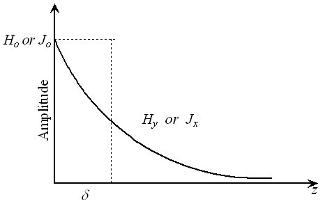
Nickel-gold plating copper PCB traces Recently a number of customers approached us because impedance controlled tracks displayed higher losses than expected. This has been evident as the impedance test trace has sloped upwards across the tested area. While on fine line traces it is quite normal to see a gently sloping trace, the level of slope (and hence loss) was much higher than predicted – so much so that Polar decided to investigate further. Eventually we discovered that the entire length of the trace had been nickel plated in the cases we investigated. While nickel is acceptable on short lengths of pad to accommodate gold plating, plating the whole trace length is generally not a good idea. This application note explains the effect that nickel will have on high frequency transmission lines. Components are normally connected to microwave circuits by soldering, or by using wire bonds onto the PCB trace. The processes used will be decided by the circuit bandwidth and operating frequency and whether assembly is automated. The most popular plating finish has historically been solder plating because of its ease of use in standard reflow soldering. However an increasing move to lead free process with no one clear ideal replacement for traditional finishes has meant that industry is going down several routes to look for alternatives. Plating finishes Other plating finishes are used, most commonly gold. However, copper and gold tend to undergo solid state diffusion into each other (with copper doing so at a faster rate); the process is accelerated by increased temperature. Copper on a trace surface oxidizes, resulting in increased contact resistance (copper migrating into the gold can cause the gold to tarnish and corrode). This can be minimized by plating a barrier layer between the copper and gold. Nickel is commonly used as a barrier layer to prevent the gold migrating into the copper on the tracks. (The nickel barrier helps to reduce both the number and the effect of pores compared with plating gold directly over the copper base.) The nickel protective coating provides several benefits. It serves as a backing to the gold for extra hardness as well as providing an effective diffusion barrier layer between gold and copper. The nickel/gold provides a finish that is heat and corrosion resistant, environmentally stable, wire solderable and durable (the nickel underplate enhances the wear characteristics of gold) albeit at a higher cost than simple solder finishes. Traditionally, nickel/gold plating has been applied over copper tracks used for keyboard contacts or edge fingers to provide the conductive, corrosion resistant coating. This approach provides benefits for soldering, but at higher frequencies the presence of the nickel layer can produce additional loss due to skin effect. The skin effect Skin effect refers to the phenomenon where electromagnetic fields (and hence the current) decay rapidly with depth inside a conductor. The diagram above graphs the amplitude of magnetic field against depth (z) into a conductor and shows the variation of the amplitude of magnetic field Hy in the z-direction where H0 is the amplitude at the conductor surface. As a consequence of Ampere's Law in a conductor, a conduction current is associated with Hy. This current will be perpendicular to Hy. Thus there is a conduction current of density Jx (where J0 is the current density at the surface) whose amplitude will vary in the same manner as that for Hy. The distance d is the value of z at which |Jx| = J0/e. This is also the same value at which the rectangular area δJ0 in the diagram equals the area under the exponential curve. δ is known as the Skin Depth. This means that most current at high frequencies flows in the outside of the conductor (in a very narrow skin on the conductor — hence the name), which in the case of nickel plated copper concentrates most of the current in the relatively lossy nickel. Nickel is a ferromagnetic material and its magnetic permeability results in a higher skin effect resistance than that of copper. In other words the skin-effect resistance on the upper (nickel plated) surface of the trace will be much higher than that of the (copper) core side. Additionally, copper's resistivity (at room temperature) is 1.7 x 10⁻⁸ ohm metre, with that of nickel over four times greater at 7 x 10⁻⁸ ohm metre. |
|
Current distribution at high frequencies At low frequencies current in a conductor follows the path of least resistance, at high frequencies it follows the path of least inductance (inductive impedance increases with frequency.) At high frequencies the distribution of current around the pcb trace is largely unaffected by the difference in skin effect resistance of the different trace metals. Resistive trace loss in nickel will be several times that in copper (in the region of three times as great at frequencies around 1GHz). Resistive loss in a conductor causes a rising slope in a TDR waveform. Any series resistance will appear as a ramp in the TDR waveform with impedance increasing linearly with distance. Series resistance simply adds to the characteristic impedance over the length of the waveform. The DC resistance of the trace combines with the high frequency skin effect to reduce the effective cross-sectional area of the trace. (In some items of TDR measuring equipment, series loss can be compensated for by adjusting the slope of the waveform by a specified number of ohms/horizontal unit. This cancels out the series resistance leaving the true characteristic impedance displayed. The Polar Controlled Impedance Test System provides compensation for this effect. Series loss may be distinguished from the case of a slightly tapered track by testing from both ends of the trace. In the case of series loss the impedance waveform will appear to have the same rising slope when tested from either end.) Selective nickel plating The cost of nickel plating, then, is a reduction in usable pcb trace length. The effective usable length of a PCB trace at high frequencies is roughly inversely proportional to the resistive trace loss. At or around 1GHz nickel plating a PCB microstrip trace reduces the useful length of the trace by a factor of three. The effect can be minimised by selective plating with nickel and gold, arranging that only pads and edge contacts of the circuit are plated. |