|
|
|
|
|
|
Enhanced modelling of solder mask coatings with the Si8000m
Application Note AP176
|
|
Impedance modelling You probably already know that it is harder to achieve a tight tolerance for impedance controlled tracks on outer layers. These screen shots demonstrate how the modelling on the Polar Si8000m multiple dielectric boundary element field solver offers a significant enhancement over the Polar Si6000 when trying to predict the finished impedance of surface microstrips. Si6000 and Si8000m coated microstrip models The following series of pictures shows the differences between the modelling employed on the Si6000 and the Si8000m. |
|
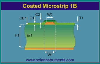
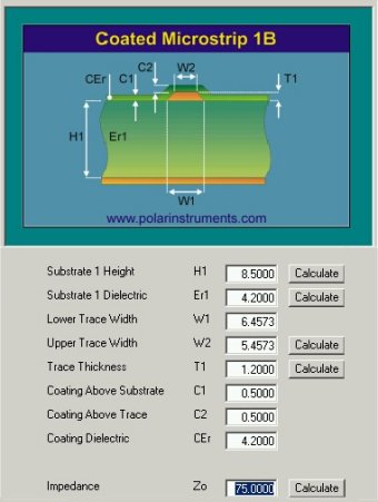
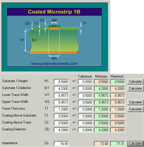
Si8000m Coated Microstrip 1B model
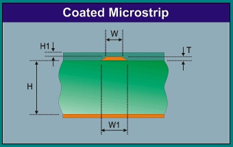
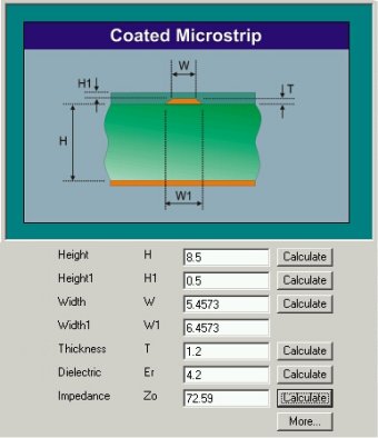
Si6000 Coated Microstrip model |
|
Note how the Si8000m boundary element field solver takes into account the profile of the solder mask. Enhanced calculation with the Si8000m Now compare the two predictions for a 75 Ohm trace: |
|
Si8000m enhanced model
The Si6000 calculates 2.4 Ohms low compared with the more accurate model in the Si8000m |
|
Modelling the production process window Finally, you can also use the Extended Interface Style of the Si8000m to display a process window, and at a glance see how production process may influence your production yield. Selecting the Extended Interface Style displays additional fields, Tolerance, Minimum and Maximum so you can specify a range of values for each parameter and observe the effect of manufacturing process variations.
Fields which control the maximum impedance value are shown in green, fields which control the minimum impedance value are shown in orange. In the example above the minimum values of trace width, W1 and W2 (shown in green) control the maximum value of impedance. Note the variation in impedance for ± 0.5 mil of etch variation. |