|
|
|
|
|
|
Surface roughness of copper effect on insertion loss
Application Note AP8155
|
NOTE: Roughness modeling and the Polar Si9000e 2017 onwards Before getting into the detail of this application note, a brief mention that the Polar Si9000e field solver offers modeling for smooth copper plus a range of methods for predicting the additional attenuation owing to surface roughness. Hammerstad is perhaps the most known, and dates from the 1940s where RF engineers needed to estimate the effects of regular roughness resulting from machining marks in the metal. This method has held up well and is effective in lines running up to data rates of around 4GHz. It also benefits from simple RMS roughness as an input parameter. A slight enhancement on this is the Groisse method, also using RMS roughness. For a model that does not saturate with frequency and for todays higher data rates the Huray method is preferred; however, this requires more complex input parameters – derived from SEM imaging. In an attempt to make this process more straightforward, many designers and OEMs have proprietary empirical methods to convert a simple RMS figure to the snowball radius / count and area required for the Huray method. (See further notes at end of this note regarding settings for Huray) Surface roughness effect on PCB trace attenuation / loss The thermal stability (and hence the reliability) of a PCB structure will relate to the mechanical strength of the bond between dielectric and copper layers. In order to provide good adhesion between copper and dielectric materials in core layers PCB materials vendors control the roughness of the associated copper layers (typically by chemical treatment). Since the roughness is a random quantity it is commonly specified in terms of the rms (root mean square) height h of the surface unevenness. The surface roughness of the copper layers will have no effect on current at low frequencies as, at low frequencies, the depth of current penetration will exceed the value of h. At high frequencies, however (i.e. in the GHz region), the skin effect (see below) will be significant as, at high frequencies, most current flows in the outside of the conductor (in a very narrow skin on the conductor — hence the name.) The skin effect Skin effect refers to the phenomenon where electromagnetic fields (and hence the current) decay rapidly with depth inside a conductor
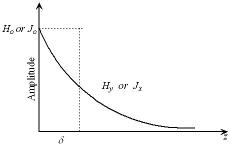
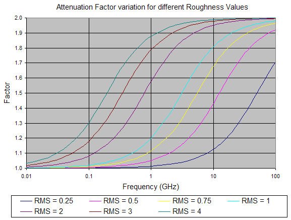
The diagram above graphs the amplitude of magnetic field against depth (z) into a conductor and shows the variation of the amplitude of magnetic field Hy in the z-direction where H0 is the amplitude at the conductor surface. As a consequence of Ampere's Law in a conductor, a conduction current is associated with Hy. This current will be perpendicular to Hy. Thus there is a conduction current of density Jx, (where J0is the current density at the surface) whose amplitude will vary in the same manner as that for Hy. The distance d is the value of z at which |Jx| = J0/e. This is also the same value at which the rectangular area dJ0 in the diagram equals the area under the exponential curve. d is known as the Skin Depth. Surface roughness At very high frequencies (where skin depth d is less than h, i.e even smaller than the conductor surface roughness) current follows the contours of the surface of the copper, effectively increasing the distance over which current must flow and hence the resistance of the copper. Chemical treatments producing roughness heights of several microns are typical with FR-4 dielectrics resulting in signal attenuation at high frequencies. Attenuation factor variations with frequency for different roughness values (in µm) are shown as shown in the graph below. From the chart it can be seen that as the surface roughness increases attenuation occurs at lower frequencies; at low values of roughness attenuation is insignificant below 1GHz, at higher values attenuation can begin at frequencies in the low hundreds of MHz.
Conductor losses in PCBs Losses that need to be considered by the PCB designer/fabricator can be summarised as conductor and dielectric losses. Conductor losses include DC, skin effect and surface roughness losses and the designer will need to balance the trade-off associated with foil roughness and conductor loss with the requirement for robust packaging – the challenge is to optimize conductor loss while ensuring good dielectric/foil adhesion. Designers and fabricators will need to discuss with the PCB vendor the surface treatments and dielectric materials available. Graphing loss due to surface roughness with the Si9000 Using the modified Hammerstad conductor roughness model the Si9000e allows the user optionally to include the RMS value for surface roughness in frequency dependent calculations and chart dielectric losses along with conductor losses and attenuation values that include compensation for surface roughness. Versions 11.01 and above further extend the modelling into both RLGC and S-parameter data. Values for surface roughness (obtainable in consultation with the board manufacturer) are specified in the currently chosen units.
Typical values for RMS roughness could be 0.8 µm (0.03mils) for stripline, 1.6µm (0.06mils) for surface microstrip. The Si9000 assumes losses on both sides of a copper trace.
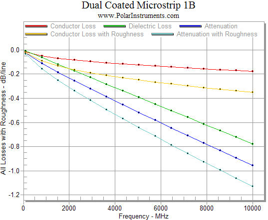
The Si9000 graph above charts all losses, the dielectric loss and the significant increase in the overall loss due to surface roughness, allowing the materials supplier to isolate the contributions of the different loss mechanisms. For designer and supplier the Si9000 will prove invaluable in recording such data to guarantee product consistency and in developing improved material behaviour. Five approaches – and guidance for use of Huray model This application note has discussed use of the Hammerstad approach for modeling surface roughness. Si9000e now allows you to choose between:
|