


The Si9000 provides for modelling plated through hole (PTH) vias with respect to impedance and signal integrity in order to allow the designer to ensure a constant impedance is presented to a signal as it propagates between devices. The Si9000 Via Checks tab includes via pad/anti-pad calculation.
The anti-pad is the void area (shown as the blue annular ring in the diagram below) between the pad and the copper of the plane. It should be designed so that it maintains the impedance of a transmission line as it passes through the plane.
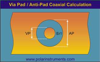
For example, assume a transmission line characteristic impedance of 50 Ohms; choose a via pad size (VP) of 12 mils (0.3mm) and calculate the anti-pad (AP) size that is required to present a nominal 50 Ohm impedance at this point.
For this calculation it is also necessary to specify the dielectric constant (Er1 illustrated above) in the region of the via. FR-4, a composite of resin (Er 3.2) and glass fibres (Er 6.1), will have a bulk Er of around 4.1 with significant local variations. It is reasonable to assume that the Er value in the immediate vicinity of the via will be lower than the bulk Er of the dielectric material as more resin will tend to flow into this type of region. In this example specify Er1 with a value of 3.5.
Enter the values of the via pad diameter, VP, of 12mil (0.3mm) and the Er1 of 3.5 into their respective fields. Move the slider bar for the anti-pad diameter, AP, until the Impedance (Zo) field displays 50 Ohms (alternatively, type the value into the Anti-Pad Diameter text box.)

Note: for this calculation the drilled size is required, not the finished size.