|
|
|
|
|
|
Speedstack – rigid PCB layer stackup design tool and documentation system
|
||||||||||||||||||||
|
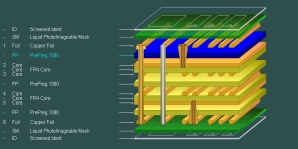
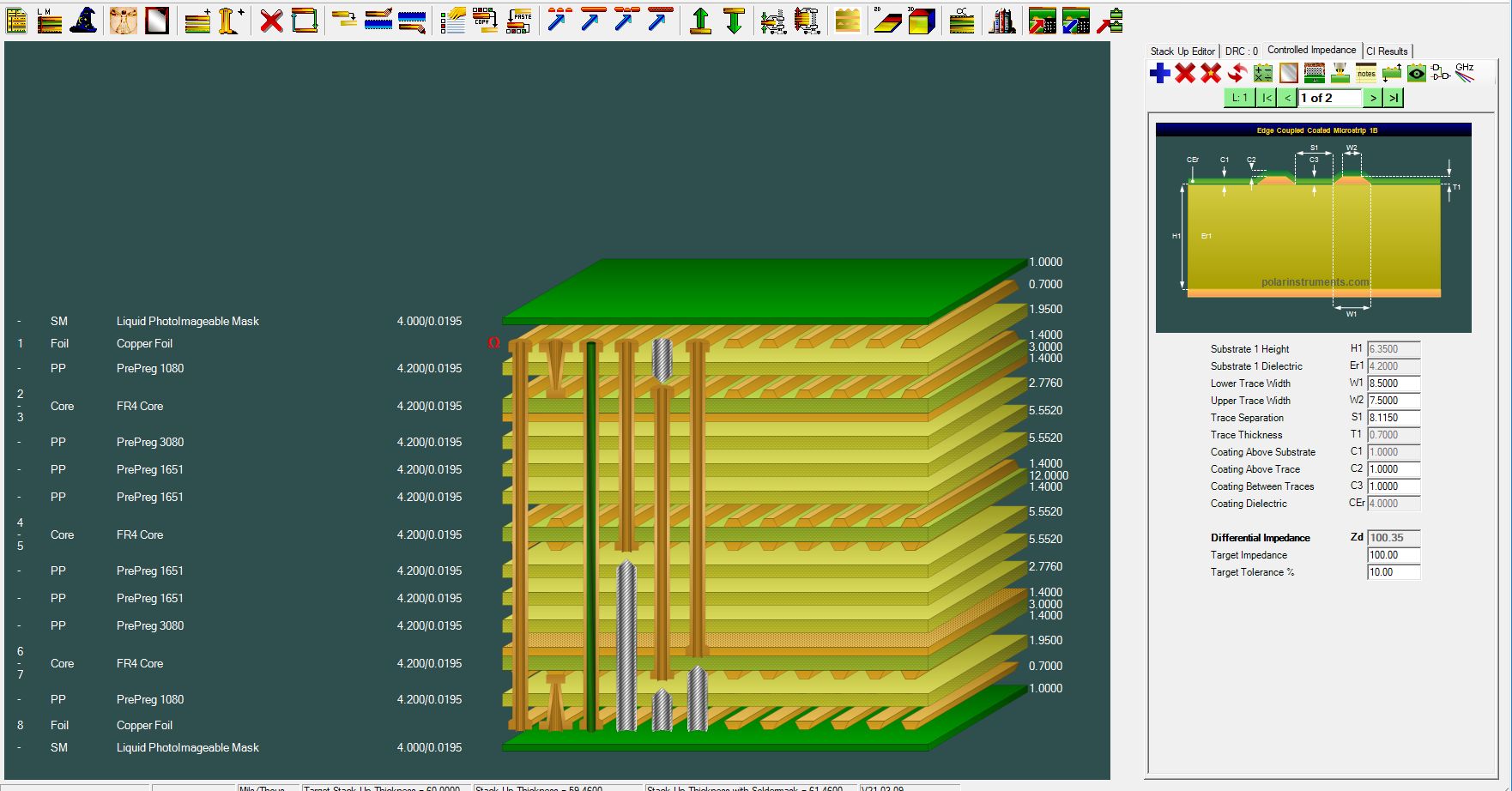
Speedstack Stackup Editor – exploded view of stackup |
||||||||||||||||||||
|
Speedstack – PCB stackup planning, design and documentation Polar's industry standard Speedstack PCB stackup design tool offers a powerful solution for PCB fabricators and designers when planning and creating live stacks – complete with controlled impedance information and professional high quality documentation.
Accessing Speedstack's online materials library Can't view the video? Click here |
||||||||||||||||||||
|
(For Flexrigid and HDI PCB stackups – see Speedstack HDI and Speedstack Flex) |
||||||||||||||||||||
|
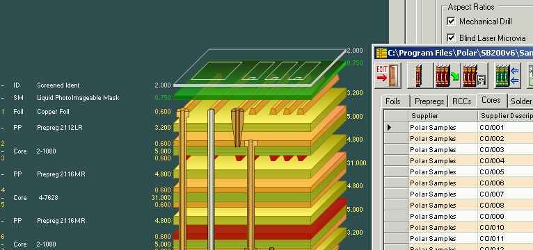
Stackup material libraries On-line material libraries Stackup material libraries for Speedstack (supplied by Polar's supplier partners listed in the Polar Materials Partner program) can be downloaded directly from the Speedstack on-line library (from Speedstack version 17:05 onwards.) On-premise material libraries Polarcare customers can request on-premise copies of the on-line libraries. Contact Polar with your Polarcare contract number and Speedstack version |
||||||||||||||||||||
|
"Thank you for the email to upgrade Speedstack and Si9000e. I have been using this toolset along with Allegro® for all my board designs. It has increased my confidence to 100% for me and my customers as I have been doing 12 and 14 layer designs. The numbers are dead on for the manufacturing group and the flow is so easy between me and my customers. Thank you again for such a wonderful toolset. Have a great day!" William Hardin PCB4Service, Inc. http://www.pcb4service.com |
||||||||||||||||||||
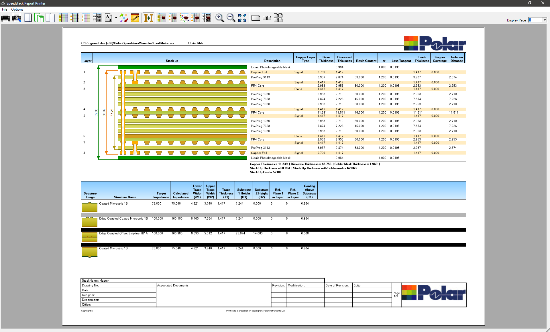
Why create your stackups with Speedstack? PCB fabricators, PCB technologists and procurement engineers are discovering that Speedstack PCB stackup design tool slashes stack creation time to a fraction of that taken by traditional methods. Designers also find that Speedstack clarifies and reduces the chances of miscommunication with PCB manufacturers and the supply chain. What exactly does Speedstack do for me? Speedstack allows you to create "live" stacks complete with controlled impedance information, either in freehand mode with Virtual Materials mode (VMM) without reference to material libraries – or from an in house material library of prepreg, core and soldermask. Speedstack takes allows you to design a stack with specifications that best meet requirements, either a general overall spec where the stack is non critical or a very detailed specification down to material types, glass styles and impedance requirements. How? You are in full control with Speedstack; you can specify the stack as tightly or loosely as you prefer. For routine builds simply enter the finished thickness and layer count and the controlled impedance specs (if any.) You can start with a generic build using virtual materials and then fine tune the stack to the level of detailed specification you require. The finished stack may then be emailed across the supply chain. The Speedstack professional report printing utility is widely acclaimed as the industry standard way to communicate stacks. Your completed stack is printed in a familiar and easy to read style. What if you continue to use informal methods for PCB stackup creation? By using informal methods for communicating stackup you risk a misunderstanding as the stack moves across the supply chain; the boards may be slightly out of specification – but still be OK, at worst the boards may be too thick for an edge connector - or have missed transmission line specs and may have to be scrapped and remanufactured. When you choose Speedstack for layerstack design and communication you will:
If you would like to learn more about Speedstack you can call or email us to talk you through the product or give you a brief web based presentation. If then you feel that there are powerful benefits for you or your organisation, your local office can set up an evaluation |
||||||||||||||||||||
|
|
|||||||||||||||||||
|
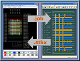
Or if you prefer to read some more – please see below: Speedstack bundles: Support and built in impedance goal seeking when used with Si8000m or Si9000e. Speedstack PCB includes Si8000m Controlled Impedance design and stackup Speedstack Si includes Si9000e Advanced PCB transmission line design and stackup Speedstack also supports optional capability for flex-rigid and HDI builds, and connects through rich XML outputs to a variety of CAD and CAM packages including Cadence Allegro (TM), Mentor Xpedition(TM), Zuken CR-8000, Ucamco Integr8tor, UCAM, and Zuken DFM center. Which version of Speedstack is right for me? Speedstack comes with a range of license packages to suit your budget... Which license is best for me? |
||||||||||||||||||||
|
||||||||||||||||||||
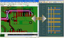
| Click picture for application view | ||||||||||||||||||||
|
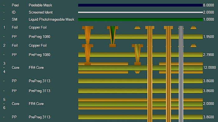
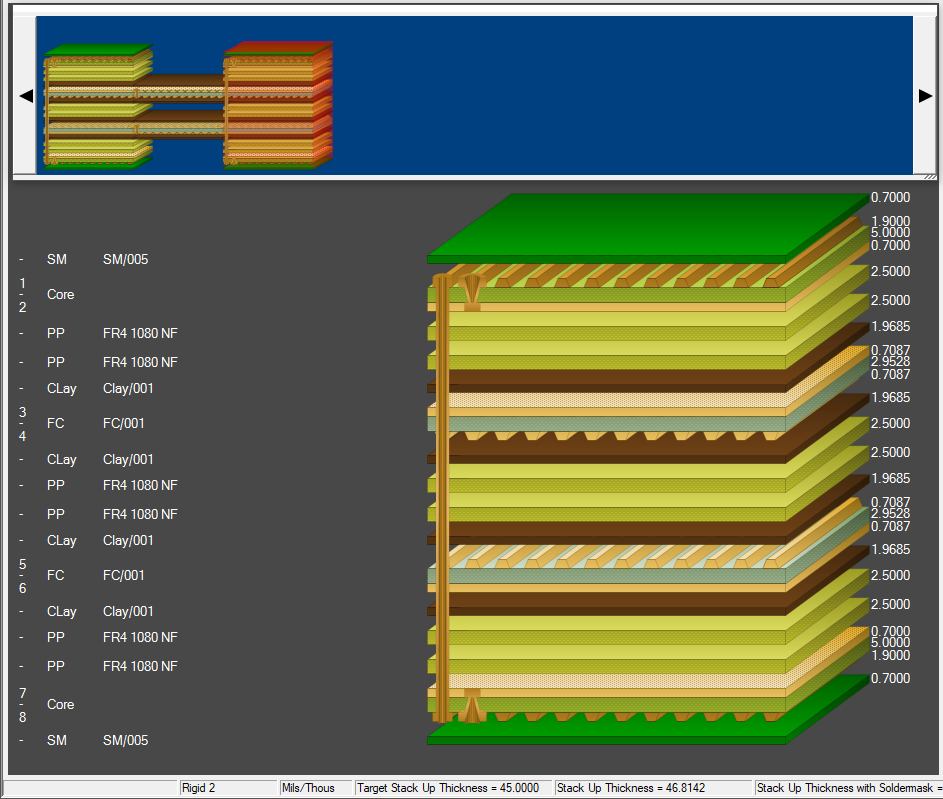
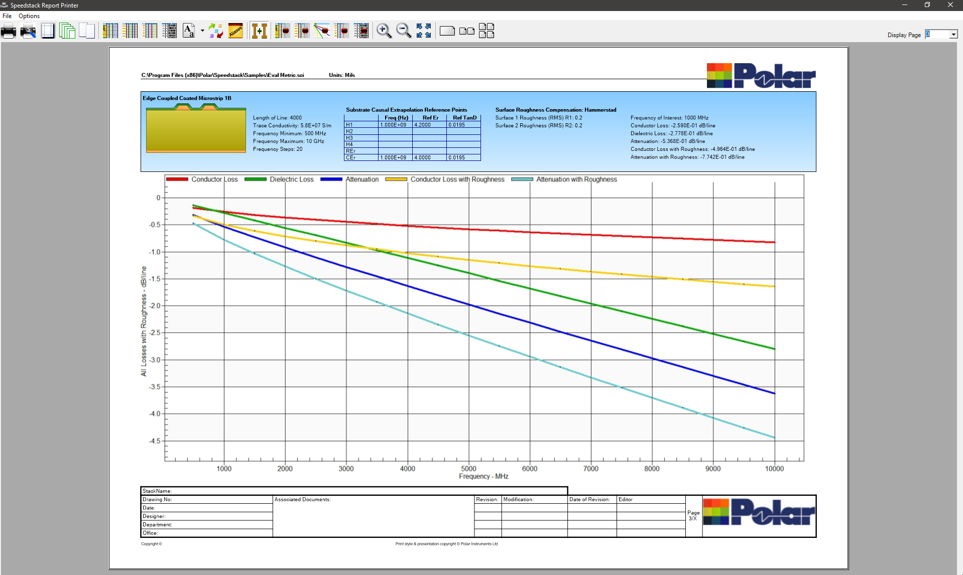
Save time PCB stackup documentation and control consumes an increasing amount of time for both interconnect designers and PCB front-end engineers. Layer build is shared using an easy to read standard format: .sci For fabricators: Now you can document layer stackup rapidly and professionally. Share material types and key stackup related information both within your facility and with your clients. For interconnect engineers: At a glance viewing of layer stackup, now you can easily communicate and share information with your preferred fabricator. For CAD department managers and PCB technologists: Are you managing multiple board vendors? Or do you simply want an error free transition from prototype to volume quantity? The Speedstack bundles all the appropriate layer stack information in an easy to digest format. For EEs: Is PCB fabrication a "black art" to you? Speedstack helps you share your requirements with your fabricator (or buyer) thus helping to ensure that you can work with your fabricator to ensure you receive boards that are both as economic as possible, whilst meeting your desired specifications. Now linking to the Si9000e PCB transmission line design system you can also extract loss / RLGC / s-parameters for your proposed stack. For buyers and brokers: As a buyer, have you ever received a batch of boards, which appeared OK, only to find that after population the production engineers come back to you complaining that a layer is swapped or the trace impedance is incorrect because of a layer stack problem? Encouraging your engineering team to supply Speedstack layer stack information files with the manufacturing data will minimise this type of unfortunate and costly mishap. Sharing stackup with Speedstack simplifies communication between the originating engineering team and the supplier(s). |
||||||||||||||||||||
|
||||||||||||||||||||
|
|
||||||||||||||||||||
|
||||||||||||||||||||
|
System requirements For PC system requirements for Speedstack see AP605 |
||||||||||||||||||||