|
|
|
|
|
|
Controlled impedance – design for test
Application Note AP132
|
|
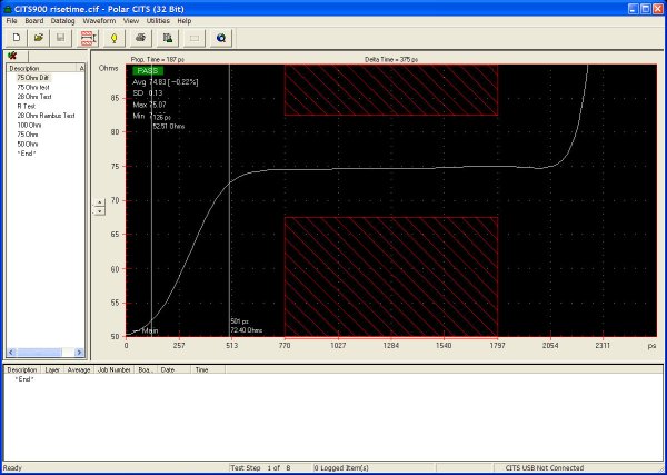
Background TDR (Time Domain Reflectometry) has become the established technique for the measurement of controlled impedance on printed circuit boards. Ideally, trace lengths of approximately 6 inches (as recommended in Standard IPC2141) allow for easy measurement, as there will be a significantly flat region of the trace to allow an accurate average impedance measurement to be made (see the impedance trace below). Designing your boards with testing in mind will assist fabricators achieve best yields and reduce the cost of your high performance boards.
Polar CITS impedance trace
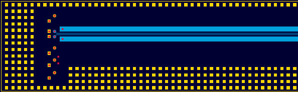
The simplest technique for PCB shops is the widely practised utilization of test coupons for verification of controlled impedance PCBs. These are either designed by the customer or added by the fabricator's front end department. Often, however, a customer will prohibit changes to the coupon. This can require the PCB fabricator to invest in a wide variety of test system probes which must be interchanged frequently, with subsequent reduction in the R&R of the measurement system. It is therefore preferable that the designer and manufacturer collaborate to modify a coupon footprint in order to minimise the number of probe variations required. Why not use variable-pitch probes? Whilst these probes are readily available, they are expensive and are designed for non-continuous operation. Variable-pitch probes are less easy for operators to use, and long term high volume use of variable-pitch probes can result in poor R&R. Make it easy for the operator As you have standardised on a coupon footprint, do ensure that all the contact points on the coupon have the same orientation. Polar's CGen Coupon Generator is designed to take impedance controlled stackup information directly from the Polar Speedstack PCB and Speedstack Si field solver and layer stackup design systems and generate the appropriate impedance test coupon containing all the required PCB controlled impedance transmission line structures.
Speedstack Coupon Generator produces coupons from existing stackup data
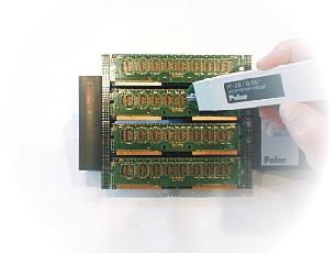
Where the coupons are built into boards, for example on Rambus® RIMM modules, test point orientation is equally important. Early RIMM designs used test points with ground positions that were 180 degrees rotated at each end of the board. Newer designs have all test points oriented in the same way. If you need to change an early Rambus design please ask us to connect you with the Rambus staff member who can confirm the change authorisation. Testing on boards Most testing is performed on coupons. If it is necessary to test traces on boards, ideally the in board coupon trace should terminate near the edge and be clearly marked. Also the via holes should be large enough to facilitate manual probing. It is almost impossible to manually TDR test on a microvia! Although the RF contact may be excellent, it is not practical to manually probe such a small contact area, especially if thousands of tests per day are required. If you need to test on actual PCB traces, then remember that the test needs to start at a net end and there must be access to ground next to the signal test point, otherwise it will not be possible to make a good RF connection to the trace under test.
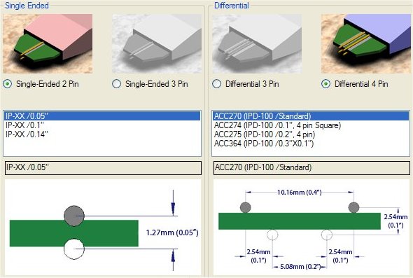
Length of test trace To obtain repeatable and consistent results in manufacturing, you need to design test traces that are of sufficient length to avoid measurement results being influenced by the effects of probe-to-trace interconnection aberrations (from the start of the trace) and pulse dispersion (which causes the trace to start to rise before the physical end of the trace.) Although some publications may recommend the specific trace region to be tested (e.g. 50% to 70%) this is not always optimum for short traces. The optimum trace length on a coupon is around 6 inches (150mm). IPC D317 contains further information on coupon design. We suggest that you select the test region by choosing the flattest, least disturbed waveform region that falls between any aberrations near the trace start and the climb towards an open circuit at the trace end. Once selected, the same region should be used for all subsequent tests of that type of PCB. Resources Sample manufacturing data for a coupon containing a wide variety of structures are available for download — (follow the link in the next paragraph). This typical coupon can be modified to suit your process and is designed with test access for both manual and automatic impedance test systems. Download sample test coupon Gerber files: mpcd1345.zip (170kb) Footprints A wide variety of probe footprints is available. You can download the latest available IP Probe Footprints for differential and single ended tests.
Polar's Coupon Generator utilises a wide range of popular probe footprints Modifying designs It is important for front end engineers to maintain a good dialog with the original designer of impedance controlled boards. Sometimes small adjustments in line width are necessary to maximise yields, or non availability of particular core or prepreg sizes may require an alteration of the stackup which will, in turn, require re-calculation of the impedance controlled dimensions. To assist in this process the Polar Speedstack PCB and Speedstack Si field solver and layer stackup design systems allows PCB designers rapidly to:
The Si8000/9000 series field solvers support single or multiple dielectric builds in a comprehensive range of trace and dielectric configurations and allow designers and board fabricators to calculate and plot impedance changes against a range of values for a specified structure parameter (charting, for example, Z0 for variations in H1, Er, etc.) The Si9000 provides for both lossless and frequency-dependent modelling and extracts full transmission line parameters (for example, RLGC matrices and 2-Port (single-ended) or 4-Port (differential) S-Parameters) for a wide range of PCB transmission lines. Graphing against frequency is provided for impedance magnitude, loss (conductor loss, dielectric loss and insertion loss), inductance, capacitance, resistance, conductance and skin depth. See also: AP124 Testing Controlled Impedance Boards with Test Coupons AP8502 Testing Controlled Impedance Boards with Test Coupons |